For my third-year computational physics project, I investigated the band structure of a strained \(\mathrm{Si}_4\mathrm{Ge}_4\) [001] superlattice: four silicon monolayers followed by four germanium monolayers, repeated along the growth direction. The question was whether layering and strain could push a silicon-based material towards a direct band gap.
Bulk silicon has an indirect band gap: the highest point in the valence band and the lowest point in the conduction band occur at different crystal momenta. This makes radiative optical transitions inefficient, which limits its usefulness in light-emitting devices. A superlattice introduces a larger real-space periodicity, changing the potential experienced by the electrons. Zone folding and strain can then shift the band structure towards more direct-gap behaviour.
I calculated the electronic band structure using an empirical pseudopotential in a plane-wave basis. Expanding the electron wavefunctions in plane waves turns the problem into a matrix eigenvalue equation. The Hamiltonian has a kinetic term and a term coupling plane waves through the crystal potential:
[
H_{\mathbf G,\mathbf G’}(\mathbf k) = \frac{\hbar^2 |\mathbf k + \mathbf G|^2}{2m}\delta_{\mathbf G,\mathbf G’} + V_{\mathbf G-\mathbf G’}.
]
The model fixes the in-plane spacing to that of a silicon substrate, compressing the germanium layers in-plane and allowing them to expand along the growth direction. After testing the plane-wave cutoff and checking the code against the free-electron limit, I searched the Brillouin zone for the valence-band maximum and conduction-band minimum, rather than relying only on the plotted high-symmetry path.
The result was an indirect gap of 0.828 eV, with the valence-band maximum at Γ and the conduction-band minimum slightly displaced along Γ–X. The lowest direct transition at Γ was 0.972 eV. Their separation is a useful measure of how close the system is to direct-gap behaviour:
[
\Delta E = E_{\Gamma}^{\mathrm{direct}} - E_{\mathrm g}^{\mathrm{indirect}}
= 0.972,\mathrm{eV} - 0.828,\mathrm{eV} = 0.144,\mathrm{eV}.
]
So the superlattice remains indirectly gapped, but lies close to the direct-gap limit. For comparison, the same model puts the direct transition in bulk silicon 2.287 eV above its indirect gap. The saved simulation run plotted below gives a gap of about 0.822 eV; the 0.828 eV quoted above is from the final report.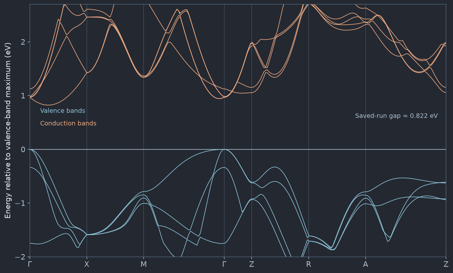 Calculated electronic bands along Γ–X–M–Γ–Z–R–A–Z.
That small separation is promising, but energetic proximity to a direct gap does not guarantee strong optical transitions. I didn’t calculate optical matrix elements or oscillator strengths, and the pseudopotential and strain model simplify what happens at the interfaces. The result is best read as an example of how strain and zone folding can change a silicon-compatible material’s electronic structure, not proof that it would make an efficient light emitter.
The full report contains the band structures and methods. Earlier in the project I investigated silicon on its own; here’s the poster and a band-structure visualisation.